RTP refers to a process that heats silicon wafers to high temperatures (up to 1200°C or greater) using high intensity lamps to set the electrical properties of the semiconductor devices.
Our thermal products now include a wide range of rapid anneals ranging from soak to spike to millisecond flash.
Our Helios family RTP systems offer unique double-side heating RTP technology. It can achieve the highest wafer temperature ramp rate while balancing wafer frontside and backside temperatures, eliminate pattern-loading effect, provide unique wafer stress management capabilities, satisfy technical requirements for RTP processes with different substrate thickness and device structures, and achieve the highest system productivity at the same time.
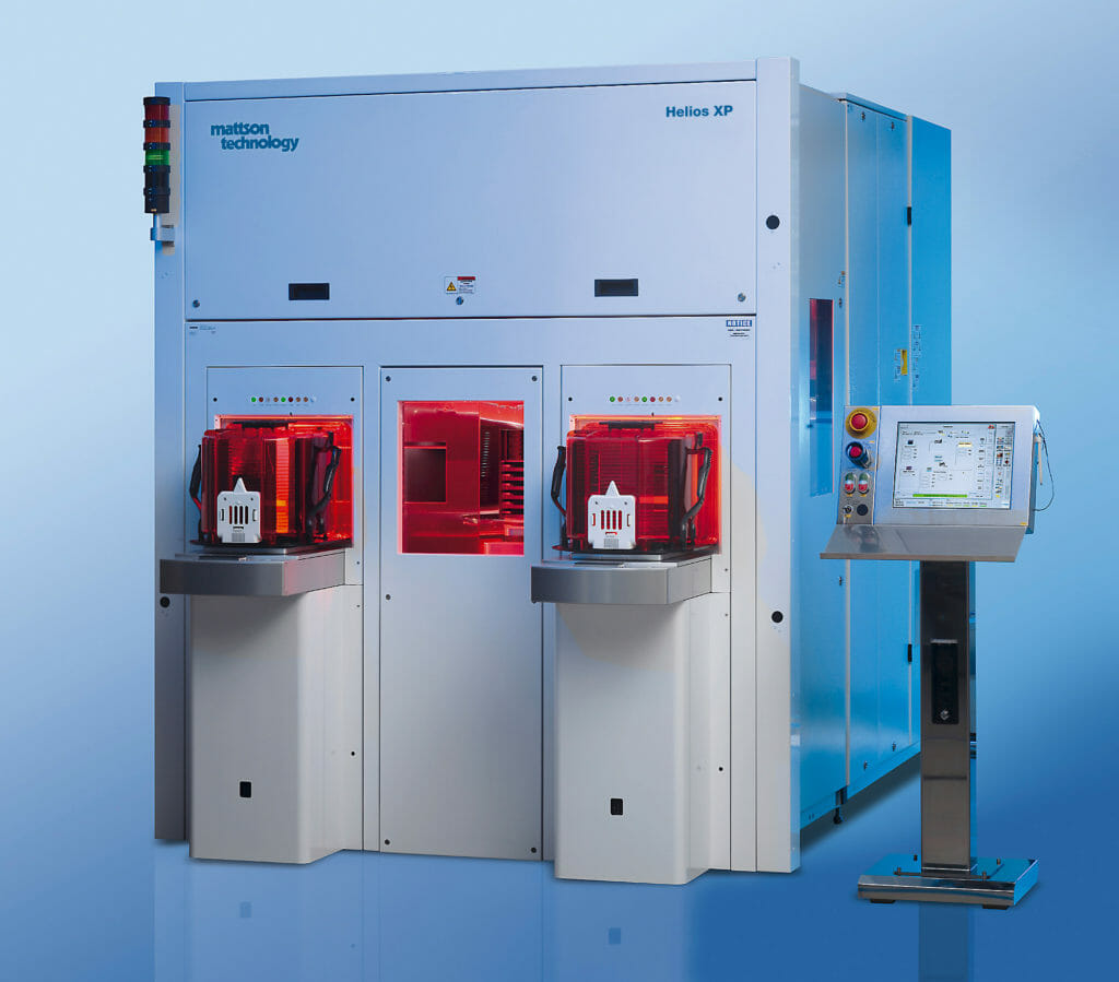
Helios® XP
The Helios XP features an advanced temperature measurement and control system combined with an active compensation algorithm for different wafer emissivities. The Helios XP can fully satisfy technical requirements in manufacturing of different semiconductor devices across various technology nodes (130 nm to 5 nm and below). The Helios XP has also demonstrated high reliability, long mean-time-between-clean, and more than 20 to 30% benefit in overall cost of ownership in mass production. It is the ideal RTP system for advanced semiconductor development and manufacturing.
Product Features and Advantages:
Superior Solution for Pattern-Loading Effect
Wafer double-side heating coupled with proven DTEC control technology
Elimination of pattern-loading effect in RTP processes
Unique Wafer Stress Management Capabilities
Wafer double-side heating for best wafer stress management
Elimination of photo-lithography defocus issue related to single-side heating
Wide RTP Applications
200°C to 1300°C temperature range, from ultra-low temperature NiSi anneal to ultra-high temperature wafer engineering
Best metal contamination performance for advanced logic device and CMOS sensor fabrication
Excellent ambient control capability, O2 < 1 ppm
High power incandescent lamp, long lifetime
High Productivity System Platform
Two process chambers
High speed wafer transfer
Small footprint
Product Applications:
Advanced logic, 3D NAND Flash Memory, DRAM
Post implant ion activation
S/D anneal
LDD anneal
Well anneal
PLAD anneal
High-k anneal
Ultra-shallow-junction formation
Metal silicide formation
Cobalt silicide formation
Nickel silicide formation
Titanium silicide formation
CMOS Sensor
Post implant ion activation
Ultra-shallow-junction formation
Metal silicide formation
Wafer Manufacturing
High temperature wafer substrate anneal
Helios® C200
The Helios C200 features an advanced temperature measurement and control system combined with an active compensation algorithm for different wafer emissivities. The Helios C200 RTP system combines superior technical performance with outstanding tool reliability. It is the ideal RTP solution for 200 mm semiconductor development and manufacturing.
Product Features and Advantages:
Unique Wafer Stress Management Capabilities
Wafer double-side heating for best wafer stress management
RTP process for different substrate thickness
Superior Solution for Pattern-Loading Effect
Wafer double-side heating coupled with proven DTEC control technology
Elimination of wafer-loading effect in RTP processes
Wide RTP Applications
200°C – 1300°C temperature range, from ultra-low temperature NiSi anneal to ultra-high temperature wafer engineering
Best metal contamination performance for CMOS sensor fabrication
 Helios® XP
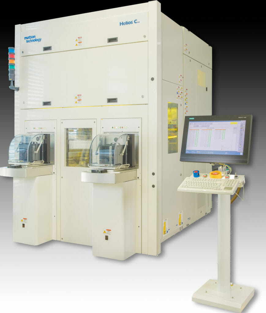 Helios® C200
 Wide RTP Applications