Dry strip is the removal of the masking layers from the wafer after the patterning process has been completed. The objective is to eliminate the masking material from the wafer as quickly as possible, without allowing any surface materials to become damaged.
We are a leader in the dry strip market. Our strip systems offer innovative wafer handling architecture to deliver low cost of ownership for integrated circuit manufacturing.
SUPREMA® product family
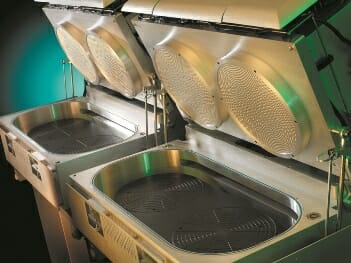
Our SUPREMA family plasma dry strip and advanced patterning film removal systems have unique ICP source and twin chamber design. Each chamber is operated independently with a dedicated vacuum transfer module for maximum process flexibility and extendibility.
The SUPREMA family plasma dry strip and advanced patterning film removal systems demonstrate high process flexibility, excellent process performance, superior particulate contamination and low cost of ownership in volume production. They are tools of choice for photoresist strip and advanced patterning film removal in semiconductor device fabrications worldwide.
Product Features and Advantages:
Remote Inductively Coupled Plasma (ICP)
Patent protected grounded Faraday shield design
High plasma density
Extraordinary reducing chemistry capability
Low particle performance
High mean-time-between-clean
Low consumable cost
Unique high fluorine process capability
Over 10,000 units installed worldwide
Twin-Wafer Chamber Design
Complete ion filtering capability
Low wafer surface plasma damage
Excellent surface integrity
Precise wafer temperature control
Full spectrum OES end point detection option
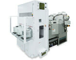
Platform
Multi-chamber design with independent vacuum transfer module
Process flexibility
Process extendibility
Process stability
Quad arm robot design, high throughput wafer transfer
Over 700 installed worldwide
Applications:
Logic / Foundry, Memory Manufacturing
Bulk strip
Post-implant strip
Strip over metal
Hardmask materials removal
Anti-reflective coating (ARC) removal
Post etch strip / clean
High aspect ratio strip / clean
Descum
COMS Image Sensor / Power Semiconductor / MEMS Manufacturing
 SUPREMA® product family