Etching is the process of selectively removing mask patterned materials from the wafer’s surface to create desired patterns on the wafer’s surface. Plasma etch is the use of a radio frequency (RF) excited plasma to produce chemically reactive species from various gases. The reactive plasma is exposed to the wafer surface and etches away the material not protected by a masking layer.
Our plasma etch products are built on our high-throughput platform to provide high overall equipment efficiency. Our plasma etch products feature proprietary Faraday shielded inductively coupled plasma (ICP) source combined with etch bias control.
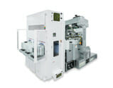 paradigmE® product family
Based on patented inductively coupled plasma (ICP) with grounded Faraday shield source designs, paradigmE plasma etch systems have unique capabilities to independently control ion energy and ion density.
paradigmE XP series products have excellent etch selectivity and low plasma damage for on-wafer devices, and are widely used for film etching in semiconductor front-end and back-end manufacturing.
paradigmE PAD series products have benefits in high etch rate, low plasma damage and low cost of consumables, and are the only ICP PAD etchers in mass production.
Our paradigmE plasma etch systems have demonstrated high performance, high reliability and low cost of ownership in leading edge memory and logic semiconductor manufacturing.